


Dr. Benjamin Klein
 Benjamin Klein received his B.S. and M.S. in Electrical Engineering from the University
of Wisconsin-Madison in 1994 and 1995, respectively. He received his Ph.D. in Electrical
Engineering from the University of Illinois – Urbana-Champaign in 2000. The subject
of his doctoral dissertation was the theory and modeling of vertical-cavity surface-emitting
lasers (VCSELs), which are a class of semiconductor laser used for telecommunications
applications.
Benjamin Klein received his B.S. and M.S. in Electrical Engineering from the University
of Wisconsin-Madison in 1994 and 1995, respectively. He received his Ph.D. in Electrical
Engineering from the University of Illinois – Urbana-Champaign in 2000. The subject
of his doctoral dissertation was the theory and modeling of vertical-cavity surface-emitting
lasers (VCSELs), which are a class of semiconductor laser used for telecommunications
applications.
From 2000-2003, Dr. Klein worked as a postdoctoral researcher at the National Institute of Standards and Technology in Boulder, Colorado, working on the modeling and design of semiconductor quantum-dot based devices, including single photon emitters and single electron transistors. From 2003-2020 he was a faculty member at the Georgia Institute of Technology, first on the Savannah campus, and later in Atlanta. At the time of his departure from Georgia Tech, he was an Associate Professor and the Associate Chair for Graduate Affairs in the School of Electrical and Computer Engineering.
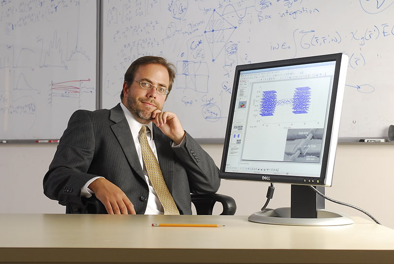
 Dr. Klein’s research interests involve the theory, modeling, and design of semiconductor
electronic and optoelectronic materials and devices. He creates and utilizes numerical
simulation programs to provide insight into the nano-scale physics of semiconductors.
He has continued his modeling work on VCSELs, and he has worked on the modeling and
design of diverse semiconductor devices including neutron scintillators, nanowire
transistors, piezo-phototronic light-emitting diodes, and plasmonic sub-wavelength
scale lasers. His most recent project is the modeling of multilayered III-nitride
samples in atom probe tomography (APT) measurement systems to assist in interpreting
the measurement data.
Dr. Klein’s research interests involve the theory, modeling, and design of semiconductor
electronic and optoelectronic materials and devices. He creates and utilizes numerical
simulation programs to provide insight into the nano-scale physics of semiconductors.
He has continued his modeling work on VCSELs, and he has worked on the modeling and
design of diverse semiconductor devices including neutron scintillators, nanowire
transistors, piezo-phototronic light-emitting diodes, and plasmonic sub-wavelength
scale lasers. His most recent project is the modeling of multilayered III-nitride
samples in atom probe tomography (APT) measurement systems to assist in interpreting
the measurement data.


